
HEAYOUNG YOON
Associate Professor
Electrical & Computer Engineering
- Associate ProfessorElectrical & Computer Engineering
- 801-585-0334 (Work)
- University of Utah, ECE, 50S. Central Campus Dr., Salt Lake City, Utah, 84112, United States
RESEARCH INTERESTS
Radial Junction Solar Cells
Sunlight is an abundant renewable energy source, providing 10,000 times more energy than the world’s current total energy use. A key metric of solar cells is power conversion efficiency, the ratio of the electrical output of a solar cell to the incident sunlight. Next generation solar cells use novel device architectures and inexpensive PV materials. For instance, an array of radial junction solar cell enables decoupling of the direction of light absorption to photo-generated carrier collection, enhancing its PV performance in comparison to planar controls.
(Image) SEM of Si Pillar Array Solar Cells

Thin-Film Solar Cells
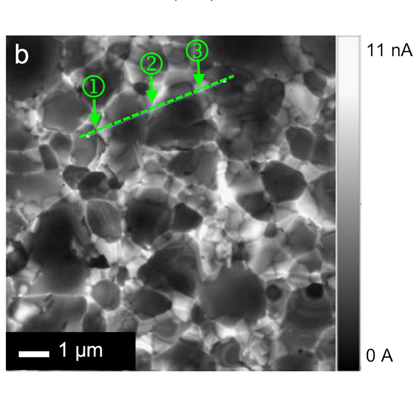
Thin film solar cells are an exciting photovoltaic (PV) technology in the market today, where a thin PV layer (< 5 µm) can absorb over 90% of sunlight. This attractive technique, however, has shown a module efficiency of 10 %, still well below the theoretical maximum value of 30 % for CdTe. It has been suggested that the absorber doping, microstructural properties (e.g., grain interior, grain boundaries), p-n junction interfaces, and/or back-contacts could be responsible for the limited performance. Our group focuses on the local PV characterizations of microstructures and correlates the inhomogeneity to device performance.
(Image) Electron Beam Induced Current (EBIC) Image of CdTe PVs
Translucent Solar Cells
Translucent solar cells are an emerging PV technology for diverse applications, including skylights, self-powered facades, sustainable urban spaces, agrovoltaics, and more. To gain widespread market acceptance, they must offer aesthetic flexibility, scalability, stability, and performance. Current methods using band-gap engineering or PV absorber thickness produce specific colors, while organic molecules or polymers degrade over time. Our research seeks to advance neutral-colored translucent PVs through scalable patterning techniques and a fundamental knowledge of photocarrier dynamics in patterned devices.

Multi-Probe Microscopy
The capability to access individual micro/nano structures and to measure their properties is critical for advanced technologies. We develop new characterization techniques by unparalleled integration of micro/nano materials (e.g., quantum dots, nanowires, 2D materials). Our team also focuses on quantitative analysis to reveal fundamental carrier dynamics at the level of individual nanostructures.
Molecular Junction Devices
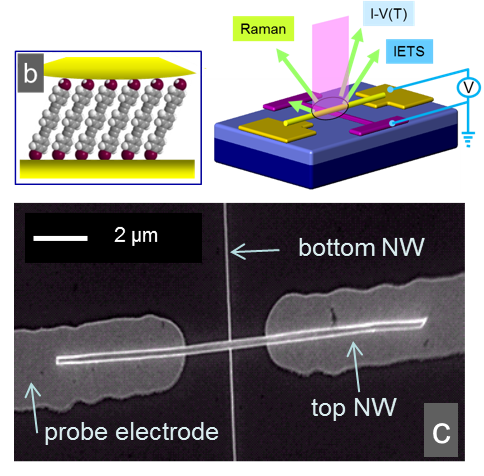
The use of self-assembled monolayer in advanced (opto)electronic devices provides a whole new degree of freedom to integrate hetero-structural nanomaterials in 3D. An example includes molecular junction devices, where the integration strategy combined a high yield parallel assembly of individually addressable devices with a technique that does not damage the active molecular units during the fabrication. Furthermore, the robust device platform allows in-situ electrical and spectroscopic characterizations to correlate between the electrical properties of the device and the structure of molecules participating in the charge transport using Raman and inelastic electron tunneling spectroscopies.
GRANTS
- EXTERNAL GRANT OR CONTRACTHIGH-POWER RADIOVOLTAIC DEVICES9 Feb 2026 - 8 Feb 2029